Featured post

Top 5 books to refer for a VHDL beginner

VHDL (VHSIC-HDL, Very High-Speed Integrated Circuit Hardware Description Language) is a hardware description language used in electronic des...

Wednesday 16 April 2014

Intel’s e-DRAM

When Intel launched their Haswell series chips last June, they stated that the high-end systems would have embedded DRAM, as a separate chip in the package; and they gave a paper at the VLSI Technology Symposium that month, and another at IEDM.
It took us a while to track down a couple of laptops with the requisite Haswell version, but we did and now we have a few images that show it’s a very different structure from the other e-DRAMs that we’ve seen.
IBM has been using e-DRAM for years, and in all of their products since the 45-nm node. They have progressed their trench DRAM technology to the 22-nm node [3], though we have yet to see that in production.Embedded DRAM in IBM Power 7+ (32-nm)
TSMC and Renesas have also used e-DRAM in the chips they make for the gaming systems, the Microsoft Xbox and the Nintendo Wii. They use a more conventional form of memory stack with polysilicon wine-glass-shaped capacitors. TSMC uses a cell-under-bit stack where the bitline is above the capacitors, and Renesas a cell-over-bit (COB) structure with the bitline below.
Embedded DRAM in Microsoft Xbox GPU fabbed by TSMC (65-mm)
Embedded DRAM in Nintendo Wii U GPU fabbed by Renesas (45-mm)
Intel also uses a COB stack, but they build a MIM capacitor in the metal-dielectric stack using a cavity formed in the lower metal level dielectrics. The part is fabbed in Intel’s 9-metal, 22-nm process:
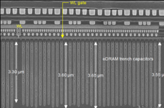
General structure of Intel’s 22-nm embedded DRAM part from Haswell package
When we zoom in and look at the edge of the capacitor array, we can see that the M2 – M4 stack has been used to form the mould for the capacitors.Intel’s-22-nm-embedded-DRAM-stack
Looking a little closer, we can see the wordline transistors on the tri-gate fin, with passing wordlines at the end of each fin. Two capacitors contact each fin, and the bitline contact is in the centre of the fin.A closer look at the Intel 22-nm embedded DRAM stack
We can see some structure in the capacitors, but at the moment we have not done any materials analysis.  A beveled sample lets us view the plan-view:
Plan-view image of the Intel 22-nm embedded DRAM capacitors
The capacitors are clearly rectangular, but again in the SEM we cannot see any detailed structure. We’ll have to wait for further analysis with the TEM for that!
Intel claims a cell capacitance of more than 13 fF and a cell size of 0.029 sq. microns, so about a third of their 22-nm SRAM cell area of ~0.09 sq. microns, and a little larger than the IBM equivalent of 0.026 sq. microns. The wordline transistors are low-leakage trigate transistors with an enlarged contacted gate pitch of 108 nm (the minimum CGP is 90 nm). In the Haswell usage the die is used as a 128 MB L4 cache, with a die size of ~79 sq. mm, co-packaged with the CPU.
Intel got out of the commodity DRAM business almost thirty years ago; it will be interesting to see where they take their new entry, though not likely into competition with the big three suppliers. Their “Knights Landing” high-performance computing (HPC) platform is reported to use 16 GB of eDRAM, which will take the equivalent of 128 of these chips, so perhaps the future is in HPC and gaming systems such as the one we bought to get the part.


Saturday 5 April 2014

Latch Up In CMOS

What is latch up in CMOS design and ways to prevent it?

A Problem which is inherent in the p-well and n-well processes is due to relatively large number of junctions which are formed in these structures, the consequent presence of parasitic diodes and transistors.

Latch-up is a condition in which the parasitic components give rise to the Establishment of low resistance conducting path between VDD and VSS with Disastrous results

Latch-up may be induced by glitches on the supply rails or by incident radiation.

Latch-up pertains to a failure mechanism wherein a parasitic thyristor (such as a parasitic silicon controlled rectifier, or SCR) is inadvertently created within a circuit, causing a high amount of current to continuously flow through it once it is accidentally triggered or turned on. Depending on the circuits involved, the amount of current flow produced by this mechanism can be large enough to result in permanent destruction of the device due to electrical overstress (EOS).

Preventions for Latch-Up

  • by adding tap wells, for example in an Inverter for NMOS add N+ tap in n-well and connect it to Vdd, and for PMOS add P+ tap in p-substrate and connect it to Vss.
  • an increase in substrate doping levels with a consequent drop in the value of  Rs.
  • reducing Rp by control of fabrication parameters and by ensuring a low contact resistance to Vss.
  • and the other is by introducing of guard rings.....

Latchup in Bulk CMOS

A byproduct of the Bulk CMOS structure is a pair of parasitic bipolar transistors. The collector of each BJT is connected to the base of the other transistor in a positive feedback structure. A phenomenon called latchup can occur when (1) both BJT's conduct, creating a low resistance path between Vdd and GND and (2) the product of the gains of the two transistors in the feedback loop, b1 x b2, is greater than one. The result of latchup is at the minimum a circuit malfunction, and in the worst case, the destruction of the device.
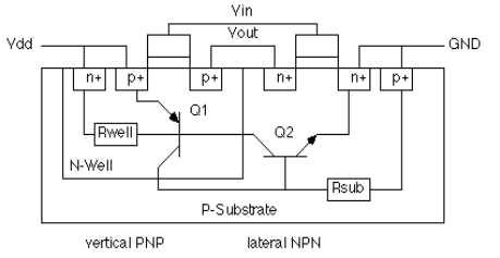
parasitic_transitor_in_bulk_cmos  Cross section of parasitic transistors in Bulk CMOS

parasitic_transitor_in_bulk_cmos_equivalent_circuit Equivalent Circuit

Latchup may begin when Vout drops below GND due to a noise spike or an improper circuit hookup (Vout is the base of the lateral NPN Q2). If sufficient current flows through Rsub to turn on Q2 (I Rsub > 0.7 V ), this will draw current through Rwell. If the voltage drop across Rwell is high enough, Q1 will also turn on, and a self-sustaining low resistance path between the power rails is formed. If the gains are such that b1 x b2 > 1, latchup may occur. Once latchup has begun, the only way to stop it is to reduce the current below a critical level, usually by removing power from the circuit.

The most likely place for latchup to occur is in pad drivers, where large voltage transients and large currents are present.

Preventing latchup

Fab/Design Approaches:

  1. Reduce the gain product b1 x b1
  • move n-well and n+ source/drain farther apart increases width of the base of Q2 and reduces gain beta2 ­> also reduces circuit density
  • buried n+ layer in well reduces gain of Q1

    2. Reduce the well and substrate resistances, producing lower voltage drops

· higher substrate doping level reduces Rsub

· reduce Rwell by making low resistance contact to GND

· guard rings around p- and/or n-well, with frequent contacts to the rings, reduces the parasitic resistances.

cmos_transitor_with_guard_rings CMOS transistors with guard rings

Systems Approaches:

  1. Make sure power supplies are off before plugging a board. A "hot plug in" of an unpowered circuit board or module may cause signal pins to see surge voltages greater than 0.7 V higher than Vdd, which rises more slowly to is peak value. When the chip comes up to full power, sections of it could be latched.
  2. Carefully protect electrostatic protection devices associated with I/O pads with guard rings. Electrostatic discharge can trigger latchup. ESD enters the circuit through an I/O pad, where it is clamped to one of the rails by the ESD protection circuit. Devices in the protection circuit can inject minority carriers in the substrate or well, potentially triggering latchup.
  3. Radiation, including x-rays, cosmic, or alpha rays, can generate electron-hole pairs as they penetrate the chip. These carriers can contribute to well or substrate currents.
  4. Sudden transients on the power or ground bus, which may occur if large numbers of transistors switch simultaneously, can drive the circuit into latchup. Whether this is possible should be checked through simulation.

Get free daily email updates!

Follow us!