When Intel launched their Haswell series chips last June, they stated that the high-end systems would have embedded DRAM, as a separate chip in the package; and they gave a paper at the VLSI Technology Symposium that month, and another at IEDM.
It took us a while to track down a couple of laptops with the requisite Haswell version, but we did and now we have a few images that show it’s a very different structure from the other e-DRAMs that we’ve seen.
IBM has been using e-DRAM for years, and in all of their products since the 45-nm node. They have progressed their trench DRAM technology to the 22-nm node [3], though we have yet to see that in production.

TSMC and Renesas have also used e-DRAM in the chips they make for the gaming systems, the Microsoft Xbox and the Nintendo Wii. They use a more conventional form of memory stack with polysilicon wine-glass-shaped capacitors. TSMC uses a cell-under-bit stack where the bitline is above the capacitors, and Renesas a cell-over-bit (COB) structure with the bitline below.
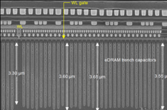
Intel also uses a COB stack, but they build a MIM capacitor in the metal-dielectric stack using a cavity formed in the lower metal level dielectrics. The part is fabbed in Intel’s 9-metal, 22-nm process:
When we zoom in and look at the edge of the capacitor array, we can see that the M2 – M4 stack has been used to form the mould for the capacitors.

Looking a little closer, we can see the wordline transistors on the tri-gate fin, with passing wordlines at the end of each fin. Two capacitors contact each fin, and the bitline contact is in the centre of the fin.

We can see some structure in the capacitors, but at the moment we have not done any materials analysis. A beveled sample lets us view the plan-view:
The capacitors are clearly rectangular, but again in the SEM we cannot see any detailed structure. We’ll have to wait for further analysis with the TEM for that!
Intel claims a cell capacitance of more than 13 fF and a cell size of 0.029 sq. microns, so about a third of their 22-nm SRAM cell area of ~0.09 sq. microns, and a little larger than the IBM equivalent of 0.026 sq. microns. The wordline transistors are low-leakage trigate transistors with an enlarged contacted gate pitch of 108 nm (the minimum CGP is 90 nm). In the Haswell usage the die is used as a 128 MB L4 cache, with a die size of ~79 sq. mm, co-packaged with the CPU.
Intel got out of the commodity DRAM business almost thirty years ago; it will be interesting to see where they take their new entry, though not likely into competition with the big three suppliers. Their “Knights Landing” high-performance computing (HPC) platform is reported to use 16 GB of eDRAM, which will take the equivalent of 128 of these chips, so perhaps the future is in HPC and gaming systems such as the one we bought to get the part.


No comments:
Post a Comment
Please provide valuable comments and suggestions for our motivation. Feel free to write down any query if you have regarding this post.