Featured post

Top 5 books to refer for a VHDL beginner

VHDL (VHSIC-HDL, Very High-Speed Integrated Circuit Hardware Description Language) is a hardware description language used in electronic des...

Monday 5 October 2015

IBM steps forward to replace Silicon Transistors with Carbon Nanotubes

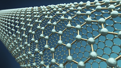
Carbon Nanotube
Carbon Nanotube
The breakthrough is that - IBM improves carbon nanotube scaling below 10nm. How ever before calling it as breakthrough we should also check out what other giants like Intel, AMD, TSMC or Samsung is working on. This breakthrough has relation with the Moore's Law. Yes you got right..!!It says that the transistor counts double only every 18 month or so. It’s the time that Intel marks 40 years of the 4004 microprocessor and here now lying some fear that progress will soon hit a wall.

You can refer to my post History and Evolution of Integrated Circuits where it shows clear progress of semiconductor industry.

But not to worry, IBM has developed a way that could help the semiconductor industry continue to make ever more dense chips to support Moore's law. These chips will be both faster and more power efficient.

Few glimpse of carbon nanotube transistors

  • Carbon nanotube transistors can operate at ten nanometers
  • Equivalent to 10,000 times thinner than a strand of human hair
  • Less than half the size of today’s leading silicon technology
  • Could also mean wearables that attach directly to skin and internal organs


Here I have an animation for Animated Nanofactory in Action.

As a result of this the devices will become smaller, increased contact resistance for carbon nanotubes has hindered performance gains until now.

These results could overcome contact resistance challenges all the way to the 1.8 nanometer node – four technology generations away.

A project at IBM is now aiming to have transistors built using carbon nanotubes ready to take over from silicon transistors soon after 2020. According to the semiconductor industry’s roadmap, transistors at that point must have features as small as five nanometers to keep up with the continuous miniaturization of computer chips.

IBM has previously shown that carbon nanotube transistors can operate as excellent switches at channel dimensions of less than ten nanometers – the equivalent to 10,000 times thinner than a strand of human hair and less than half the size of today’s leading silicon technology.

IBM's new contact approach overcomes the other major hurdle in incorporating carbon nanotubes into semiconductor devices, which could result in smaller chips with greater performance and lower power consumption.

Earlier this summer, IBM unveiled the first 7 nanometer node silicon test chip, pushing the limits of silicon technologies and ensuring further innovations for IBM Systems and the IT industry.

By advancing research of carbon nanotubes to replace traditional silicon devices, IBM is paving the way for a post-silicon future and delivering on its $3 billion chip R&D investment announced in July 2014.

IBM’s chosen design uses six nanotubes lined up in parallel to make a single transistor. Each nanotube is 1.4 nanometers wide, about 30 nanometers long, and spaced roughly eight nanometers apart from its neighbors. Both ends of the six tubes are embedded into electrodes that supply current, leaving around 10 nanometers of their lengths exposed in the middle. A third electrode runs perpendicularly underneath this portion of the tubes and switches the transistor on and off to represent digital 1s and 0s.

The IBM team has tested nanotube transistors with that design, but so far it hasn't found a way to position the nanotubes closely enough together, because existing chip technology can’t work at that scale. The favored solution is to chemically label the substrate and nanotubes with compounds that would cause them to self-assemble into position. Those compounds could then be stripped away, leaving the nanotubes arranged correctly and ready to have electrodes and other circuitry added to finish a chip.

Sunday 4 October 2015

International Conference on VLSI Design and Embeded Systems - Jan 2016


Friends, get yourself ready for the 29th International Conference on VLSI Design and 15th International Conference on Embedded Systems which will be held during January 4-8, 2016 at Kolkata, West Bengal, India.

The theme for the conference this year is "Technologies for a Safe and Inclusive World". This 5 day conference comprises: first three days (January 4 to 6, 2016) of main conference followed by Tutorials during the last two days (January 7-8, 2016).

The convergence of technology with modern life has reached a state where dependence of human life on semiconductor technology is ubiquitous. Today semiconductor technology is poised to look beyond its traditional bastions of application with pervasive impact on healthcare, environment, energy, transportation, and disaster management. The 29th International Conference on VLSI Design and the 15th International Conference on Embedded Systems will bring together industry and academia to present front-end technology under the theme of Technologies for a Safe and Inclusive World.

The Technical tracks will be grouped under the theme track and the three broad categories namely, Design Methodologies and Technology, Design Tools and EDA and Embedded System Design and Tools. The conference proceedings will be published by the IEEE Computer Society Press. Selected papers from this conference will also be published as special issues of top archival journals. 

Authors are invited to submit full-length (6 pages maximum) in IEEE CS proceedings format, original, unpublished papers with an abstract (200 words maximum) under the tracks listed below. To enable double blind review, the author list should be omitted from the main document. Papers violating length and blind-review criteria would be excluded from the review process. Previously published papers or papers currently under review for other conferences/journals should not be submitted and will not be considered for publication. 

Track: Design Methodology and Technology 
D1: System-level Design 
ESL, System-level design methodology, Multicore systems, Processor and memory design, Concurrent interconnect, Networks-on-chip, Defect tolerant architectures 

D2: Advances in Digital Design 
Logic and Physical synthesis; Place & Route, Clock Tree, Physical Verification, Timing and Signal integrity, Power analysis and integrity, OCV, DFM; DFY; Challenges for advanced technology nodes 

D3: Analog / RF Design 
Analog Mixed Signal IP; High-Speed interfaces; SDR and wireless; Low-power Analog and RF; Effective use of Spectrum; Memory Design, Standard Cell Design 

D4: Power Aware Design 
Low-power design, micro-architectural techniques, thermal estimation and optimization, power estimation methodologies, and CAD tools 

D5: Devices / Circuits 
New Devices and architectures; Low power devices; Modeling and Simulation; Multi-domain simulation; Numerical methods; Device/circuit level variability models; Reliability simulation 

D6: Emerging Technologies 
Nano-CMOS technologies; MEMS; CMOS sensors; CAD/EDA methodologies for nanotechnology; Nano-electronics and Nano-circuits, Nano-sensors, MEMS applications, Nano-assemblies and Devices, Non-classical CMOS; Post-CMOS devices; Biomedical circuits, Carbon Nano-tubes based computing 

Track : Design Tools and EDA 
T1: Design Verification 
Functional Verification; Behavioral Simulation; RTL Simulation; Coverage Driven Verification; Assertion Based Verification; Gate-level simulation; Emulation; Hardware Assisted Verification; Formal Verification; Equivalence Checking; Verification Methodologies 

T2: Test Reliability and Fault-Tolerance 
DFT, Fault modelling/simulation; ATPG; Low Power DFT; BIST & Repair; Delay test; Fault tolerance; Online test; AMS/RF test; Board-level and system-level test; Silicon debug, post-silicon validation; Memory test; Reliability test; static and dynamic defect- and fault-recoverability, and variation-aware design 

T3: Computer-Aided Design (CAD) 
Hardware/software co-design, logic and behavioural synthesis, logic mapping, simulation and formal verification, layout (partitioning, placement, routing, floorplanning, compaction) 

Track : Embedded System Design and Tools 
E1: Embedded Systems 
Hardware/Software co-design & verification; Reconfigurable computing; Embedded multi-cores SOC and systems; Embedded software including Operating Systems, Firmware, Middleware, Communication, Virtualization, Encryption, Compression, Security, Reliability; Hybrid systems-on-chip; Embedded applications, Platforms & Case studies 

E2: FPGA Design and Reconfigurable Systems 
FPGA Architecture, FPGA Circuit Design, CAD for FPGA, FPGA Prototyping 

E3: Wireless Systems 
Wireless Sensor Networks, Low Power wireless Systems, Embedded Wireless, Wireless protocols, Wireless Power / Charging 

Theme Track : Technologies for a Safe and Inclusive World 
H1: Technologies for Healthcare Applications 
H2: Technologies for Smart Management of Energy Systems 
H3: Technologies for Intelligent and Secure Transportation Systems 
H4: Technologies for Safety Assurance of Embedded Circuits and Systems 
H5: Technologies for Secure Embedded Circuits and Systems 


Proposals for Tutorials and Special Sessions/Panel Discussion on the above-listed topics (but not limited to) are invited. Please check conference website for details. 

Important dates are the following: 

REGULAR PAPERS 
Abstract submission : July 19, 2015 (Sunday) 
Full Paper submission : July 26, 2015 (Sunday) 
Acceptance Notification : Sep 26, 2015 (Saturday) 
Camera-ready version : Oct 11, 2015 (Sunday) 

TUTORIALS 
Tutorial Proposals : July 19, 2015 (Sunday) 
Acceptance Notification : Sep 26, 2015 (Saturday) 
Presentation Slides : Nov 15, 2015 (Sunday) 

SPECIAL SESSIONS 
Proposal submission : July 19, 2015 (Sunday) 
General Chairs 
Pradip Bose, IBM 
Susmita Sur-Kolay, ISI 

Vice-General Chairs 
Indranil Sengupta, IITKGP 
Parthasarathi Dasgupta, IIMC 

Program Chairs 
Krishnendu Chakrabarty, Duke 
Pallab Dasgupta, IITKGP 
Partha P. Das, IITKGP 

Tutorial Chairs 
Hafizur Rahaman, IIEST 
Prabhat Mishra, UF 
Annajirao Garimella, Intel 

Publiciy chairs 
Chandan Giri, IIESTS 
Ken Stevens, U. Utah 
Monica Pereira, UFRN 
Robert Wille, U. Bremen 
Swarup Bhunia, CWRU 
T. -Y. Ho, NCKU