Featured post

Top 5 books to refer for a VHDL beginner

VHDL (VHSIC-HDL, Very High-Speed Integrated Circuit Hardware Description Language) is a hardware description language used in electronic des...

Tuesday 27 September 2011

R-S Flip Flop

Fig 1The circuit of Fig.1 is called a SR flip-flop or bi-stable. We will consider its truth table, and immediately find that we have a problem. We can construct the table for the three states where at least one input is zero. This is because if any input to a nand gate is zero, the output will be one regardless of the other input, and we can therefore work around the loop to calculate all the values. However when R and S are 1 we cannot immediately calculate P and Q; so the only way we can analyze what happens is to look at the possible values that P and Q could hold. Thus we can expand the truth table to include a further two inputs Pp and Qp where the subscript p indicates the previous value.

S

R

Pp

Qp

P

Q


1

1

0

0

1

1

Unstable

1

1

0

1

0

1

Stable

1

1

1

0

1

0

Stable

1

1

1

1

0

0

Unstable

Here we see that there are two states where P=Pp and Q=Qp (1101 and 1110 respectively). These are therefore stable states. The other two states (1100 and 1111) are unstable, and using the simple model with time delay t will oscillate with a period of 2t. In practice, the circuit will fall into one of the two stable states rather than oscillate, since the time delays of the two nand gates will not be precisely the same. Which state if will finish in is non deterministic. In practice we are not interested in the non-deterministic states, only in the stable ones.

Fig.2This circuit can be considered to be a one bit memory circuit since Q can be set to one or zero. To see this we need to look at a sequence of inputs as shown in Fig.2. At the third time step we have the input 10 which puts the circuit into a known state and the output Q to 1. That value of Q is memorised and remains as long as the input is kept at 11. At the sixth time step the input 01 forces the output Q to be a 0, and as long as the input is held at 11 this 0 remains. This way of looking at the circuit gives rise to the names of the inputs S for Set and R for Reset, and so this flip flop is usually given the name R-S. The following three points should be noted. We are now describing the behaviour by means of a sequence of inputs, and for this reason, these circuits are referred to a sequential. Secondly, in all the cases of interest for this circuit P=Q'. Thirdly, an R-S flip flop can equivalently be built out of NOR gates.

Monday 19 September 2011

VHDL Language Reference Manual (LRM)

The VHSIC Hardware Description Language (VHDL) is a formal notation intended for use in all phases of the creation of electronic systems. Because it is both machine readable and human readable, it supports the development, verification, synthesis, and testing of hardware designs, the communication of hardware design data, and the maintenance, modification, and procurement of hardware. The form of a VHDL description is described by means of context-free syntax together with context-dependent syntactic and semantic requirements expressed by narrative rules. The context-free syntax of the language is described using a simple variant of Backus-Naur form.

DOWNLOAD VHDL LRM

Verilog language reference manual LRM

Verilog was started initially as a proprietary hardware modeling language by Gateway Design Automation Inc. around 1984. It is rumored that the original language was designed by taking features from the most popular HDL language of the time, called HiLo, as well as from traditional computer languages such as C. At that time, Verilog was not standardized and the language modified itself in almost all the revisions that came out within 1984 to 1990.
 
Verilog simulator was first used beginning in 1985 and was extended substantially through 1987. The implementation was the Verilog simulator sold by Gateway. The first major extension was Verilog-XL, which added a few features and implemented the infamous "XL algorithm" which was a very efficient method for doing gate-level simulation.
 
The time was late 1990. Cadence Design System, whose primary product at that time included Thin film process simulator, decided to acquire Gateway Automation System. Along with other Gateway products, Cadence now became the owner of the Verilog language, and continued to market Verilog as both a language and a simulator. At the same time, Synopsys was marketing the top-down design methodology, using Verilog. This was a powerful combination.
 
In 1990, Cadence recognized that if Verilog remained a closed language, the pressures of standardization would eventually cause the industry to shift to VHDL. Consequently, Cadence organized the Open Verilog International (OVI), and in 1991 gave it the documentation for the Verilog Hardware Description Language. This was the event which "opened" the language.
 
OVI did a considerable amount of work to improve the Language Reference Manual (LRM), clarifying things and making the language specification as vendor-independent as possible.
 
Soon it was realized that if there were too many companies in the market for Verilog, potentially everybody would like to do what Gateway had done so far - changing the language for their own benefit. This would defeat the main purpose of releasing the language to public domain. As a result in 1994, the IEEE 1364 working group was formed to turn the OVI LRM into an IEEE standard. This effort was concluded with a successful ballot in 1995, and Verilog became an IEEE standard in December 1995.
 
When Cadence gave OVI the LRM, several companies began working on Verilog simulators. In 1992, the first of these were announced, and by 1993 there were several Verilog simulators available from companies other than Cadence. The most successful of these was VCS, the Verilog Compiled Simulator, from Chronologic Simulation. This was a true compiler as opposed to an interpreter, which is what Verilog-XL was. As a result, compile time was substantial, but simulation execution speed was much faster.
 
In the meantime, the popularity of Verilog and PLI was rising exponentially. Verilog as a HDL found more admirers than well-formed and federally funded VHDL. It was only a matter of time before people in OVI realized the need of a more universally accepted standard. Accordingly, the board of directors of OVI requested IEEE to form a working committee for establishing Verilog as an IEEE standard. The working committee 1364 was formed in mid 1993 and on October 14, 1993, it had its first meeting.
 
The standard, which combined both the Verilog language syntax and the PLI in a single volume, was passed in May 1995 and now known as IEEE Std. 1364-1995.
 
After many years, new features have been added to Verilog, and the new version is called Verilog 2001. This version seems to have fixed a lot of problems that Verilog 1995 had. This version is called 1364-2001.
 
Timeline:
1984 Verilog-XL simulator and language developed by Gateway Design Automation
1987 Synopsys introduced a Verilog based synthesis tool.
1989 Cadence Design Systems acquired Gateway, and Verilog.
1990 Cadence placed the Verilog language in the public domain.
1995 Verilog HDL became (IEEE Std 1364-1995).
1997 Verilog VCS bought by Viewlogic
1997 Viewlogic bought by Synopsys
1998 Synopsys issues Verilog VCS
2001 A significantly revised version was published in 2001.
 

VHDL Code for Multiplxer using with-select statement

Below written VHDL code is for 4x1 multiplexer using with-select statement.

LIBRARY IEEE;
USE IEEE.std_logic_1164.ALL;

ENTITY mux4 IS
  PORT ( i0, i1, i2, i3, a, b : IN std_logic;
                            q : OUT std_logic);
END mux4;

ARCHITECTURE mux4 OF mux4 IS
  SIGNAL sel: INTEGER;
BEGIN
  WITH sel SELECT
    q <= i0 AFTER 10 ns WHEN 0,
         i1 AFTER 10 ns WHEN 1,
         i2 AFTER 10 ns WHEN 2,
         i3 AFTER 10 ns WHEN 3,
         'X' AFTER 10 ns WHEN OTHERS;

  sel <= 0 WHEN a = '0' AND b = '0' ELSE
         1 WHEN a = '1' AND b = '0' ELSE
         2 WHEN a = '0' AND b = '1' ELSE
         3 WHEN a = '1' AND b = '1' ELSE
         4 ;
END mux4;

VHDL Code for Multiplxer using When-else statement

Below written VHDL code is for 4x1 multiplexer using when-else statement.

LIBRARY IEEE;
USE IEEE.std_logic_1164.ALL;
ENTITY mux IS
  PORT (i0, i1, i2, i3, a, b: IN std_logic;
        q : OUT std_logic);
END mux;

ARCHITECTURE bad OF mux IS
BEGIN
  q <= i0 WHEN a = '0' AND b = '0' ELSE '0';
  q <= i1 WHEN a = '1' AND b = '0' ELSE '0';
  q <= i2 WHEN a = '0' AND b = '1' ELSE '0';
  q <= i3 WHEN a = '1' AND b = '1' ELSE '0';
END BAD;

ARCHITECTURE better OF mux IS
BEGIN
  q <= i0 WHEN a = '0' AND b = '0' ELSE
       i1 WHEN a = '1' AND b = '0' ELSE
       i2 WHEN a = '0' AND b = '1' ELSE
       i3 WHEN a = '1' AND b = '1' ELSE
       'X';      --- unknown
END better;

Friday 16 September 2011

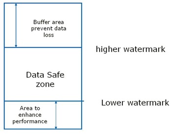
How to decide FIFO depth?

It is an interesting Architectural decision, what should be our FIFO depth?

  • What is the Transmitter data rate?
  • What is the receiver data rate?

when there is a requirement for FIFO? when the Transmitter data rate and the receive data rate are not in sync rather they don't match.

The read is slower than the write, so there is always a chance the data will be lost, so FIFO will be an intermediate logic where the data would be buffered or stored .

smaller FIFO depth can cause overflow scenario and cause a data loss

Possible scenario's:

Scenario 1:

Write is in maximum condition & Read is in minimum condition, means Write process is writing the data faster and read is reading or accessing the data slowest.

Scenario 2:

Whether the design supports only single writes or burst writes also. It becomes more complex when burst writes are present.

Scenario 3:

Write with no idle cycles and read with idle cycles.

Scenario 4:

Is the design requirement is of Synchronous FIFO or an asynchronous FIFO?

Synchronous FIFO: A First In First Out memory, where in the has a control logic mechanism, has read and write pointers, generates Status signals and places handshake signals across. Sync FIFO has a same clock frequency for both read and write operation.

The control/status signals could be Read Error, Write Error signals generated. Read Error generated when the FIFO is empty and Write Error is generated when the FIFO is full, writing may cause a data loss.Based on these signals can generate interrupt signals to act upon. Handshake signals could be Read Enable or a Write Enable, Write Acknowledge and read acknowledge.

Asynchronous FIFO: The operation of Write and Read of a FIFO is purely asynchronous.

Scenario 5:

The Data width of an Tx and Rx are different.
fifo_depth