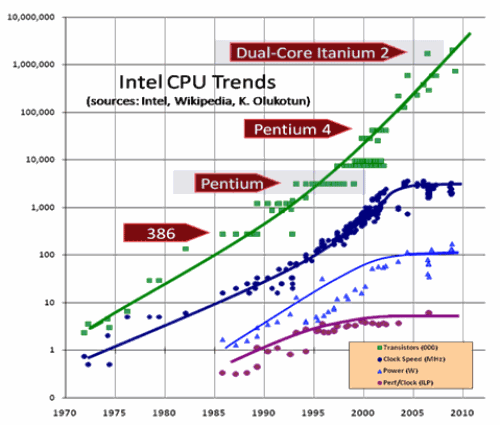
Where do we actually see VLSI in action? Everywhere, in personal computers, cell phones, digital cameras and any electronic gadget. There are certain key issues that serve as active areas of research and are constantly improving as the field continues to mature. The figures would easily show how Gordon Moore proved to be a visionary while the trend predicted by his law still continues to hold with little deviations and don’t show any signs of stopping in the near future. VLSI has come a far distance from the time when the chips were truly hand crafted. But as we near the limit of miniaturization of Silicon wafers, design issues have cropped up.
VLSI is dominated by the CMOS technology and much like other logic families, this too has its limitations which have been battled and improved upon since years. Taking the example of a processor, the process technology has rapidly shrunk from 180 nm in 1999 to 60nm in 2008 and now it stands at 45nm and attempts being made to reduce it further (32nm) while the Die area which had shrunk initially now is increasing owing to the added benefits of greater packing density and a larger feature size which would mean more number of transistors on a chip.
As the number of transistors increase, the power dissipation is increasing and also the noise. If heat generated per unit area is to be considered, the chips have already neared that of the nozzle of a jet engine. At the same time, the Voltage scaling of threshold voltages beyond a certain point poses serious limitations in providing low dynamic power dissipation with increased complexity. The number of metal layers and the interconnects be it global and local also tend to get messy at such nano levels.
Even on the fabrication front, we are soon approaching towards the optical limit of photolithographic processes beyond which the feature size cannot be reduced due to decreased accuracy. This opened up Extreme Ultraviolet Lithography techniques. High speed clocks used now make it hard to reduce clock skew and hence putting timing constraints. This has opened up a new frontier on parallel processing. And above all, we seem to be fast approaching the Atom-Thin Gate Oxide layer thickness where there might be only a single layer of atoms serving as the oxide layer in the CMOS transistors. New alternatives like Gallium Arsenide technology are becoming an active area of research owing to this.
Where does it all lead us to? The future of VLSI seems to change every little moment as we read this.
Links:


No comments:
Post a Comment
Please provide valuable comments and suggestions for our motivation. Feel free to write down any query if you have regarding this post.