One important design rule is to use only one edge of the clock signal. Although this is a good design practice in some special cases it might be helpful to use both edges.
Listing 1. not synthesizable dual-edge behavior in VHDL
process (reset, clock)
begin
if (reset = ‘1’) then
−− reset
elsif rising_edge(clock) then
−− synchronous behavior
elsif falling_edge (clock) then
−− synchronous behavior
end if;
end process;
One example is low-power signal processing, where all state machines should run at the symbol frequency to avoid unnecessary switching. But the signal frequency might be higher than the symbol frequency.
FM0 encoding (fig. 1) is an example. With FM0 encoding always the signal switches at the begin of every symbol. Another signal switch is done in the middle of the symbol, if zero has to be transmitted. If a transmitter wants so send a FM0 encoded data stream and runs only at the symbol frequency, the output signal has to be switched with the rising edge of clock and additionally with the falling edge, if zero is transmitted.
Another example for dual-edge behavior are clock dividers. For odd divisors the divided clock signal has to be switched at the falling edge of the fast clock, to get the same length for the low and the high period.
There are two problems if dual-edge behavior is desired:
- Most cell libraries do not provide a dual-edge flip-flops.
- In VHDL dual-edge behavior can be described as shown in listing 1, but most synthesis tools do not support this. Only few are capable of handling such a description. Therefore we need another way to model dual-edge behavior.
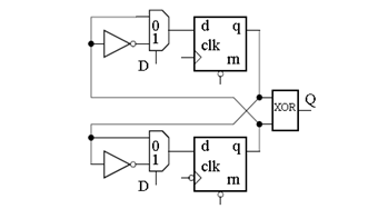
Although dual-edge behavior is not supported by VHDL, synthesis and the cell libraries, a dual-edge flipflop can be described as shown in fig. 2. Note that synthesis tools will transform the multiplexers into XOR gates.
 Fig. 2. Pseudo Dual-Edge D-Flipflop (pde dff)
The pde dff consists of 2 cross-coupled flipflops, one triggered by the rising and the other one triggered by the falling edge of the clock signal c. The outputs of the flipflops are connected via an XOR gate. Although not shown in fig. 2, asynchronous set and reset are possible.
The synthesizable VHDL source code of the pde dff is shown in listing 2. Both asynchronous set (sn) and reset (rn) can be turned on or off using generic parameters. Using both edges of the clock means doubling the clock frequency. Propagation paths have to be half as long for dualedge logic compared to common single-edge logic.
Although the pde dff looks symmetric it has in general asymmetric behavior in terms of the propagation time for the rising and the falling edge of the data output q. It depends on the data input d, the stored values in the two flip-flops and the propagation times of both the flip-flops and the final XOR gate.
For the example of FM0 encoding (fig. 1) this means that for a continuous transmission of the symbol zero in general the time of the output q being high is not equal to the time of the output being low. Such an asymmetry is not uncommon even for single-edge flipflops but for the pde dff it is slightly bigger.
Listing2. The Pseudo Dual-Edge D-FF in VHDL:
library IEEE;
use IEEE.STD_LOGIC_1164.ALL;
IEEE.Numeric_std.ALL;
entity pdedff is
generic (
impl_rn: integer := 1; −− with async reset if 1
impl_sn: integer := 1); −− with async set if 1
port(
rn:in std_ulogic; −− low−active
sn:in std_ulogic; −− low−active
d:in std_ulogic;
c:in std_ulogic;
q:out std_ulogic);
end pdedff;
−−pseudo dual−edgeD−flipflop
−−reset and set are lowactive and can be
−−(de)activated using the generic paramters
architecture behavior of pdedff is
signal ff_rise, ff_fall:std_ulogic;
begin
process(rn, sn, c)
begin
if(impl_rn=1 AND rn=’0’) then
ff_rise <= ’0’;
elsif (impl_sn=1 AND sn=’0’) then
ff_rise <= ‘1’;
elsif rising_edge (c) then
if (d= ‘1’) then
ff_rise <= NOT (ff_fall);
else ff_rise <= ff_fall;
endif;
endif;
end process;
process(rn, sn, c)
begin
if(impl_rn = 1 AND rn= ‘0’) then
ff_fall <= ‘0’;
elsif (impl_sn= 1 AND sn = ‘0’) then
ff_fall <= ‘0’;
elsif falling_edge (c) then
if (d = ‘1’) then
ff_fall <= NOT (ff_rise);
else
fffall <= ff_rise;
endif;
endif;
end process;
q <= ‘0’ when (impl_rn = 1 AND rn= ‘0’) else
‘1’ when (impl_sn= 1 AND sn= ‘0’) else
ff_rise XOR ff_fall;
−−rn and sn used to suppress spikes
endbehavior;


No comments:
Post a Comment
Please provide valuable comments and suggestions for our motivation. Feel free to write down any query if you have regarding this post.