Featured post

Top 5 books to refer for a VHDL beginner

VHDL (VHSIC-HDL, Very High-Speed Integrated Circuit Hardware Description Language) is a hardware description language used in electronic des...

Wednesday 21 January 2009

Future of VLSI


feature_of_vlsi_design 

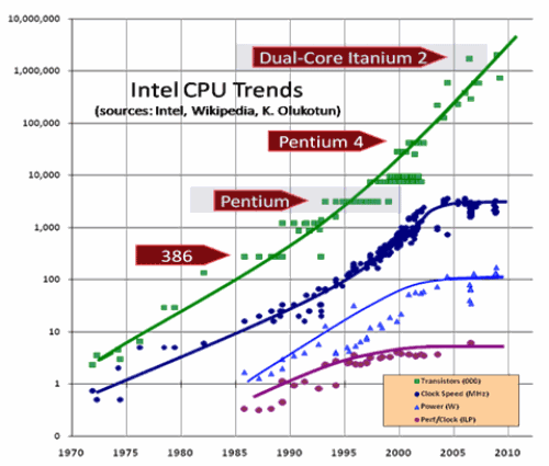
Where do we actually see VLSI in action? Everywhere, in personal computers, cell phones, digital cameras and any electronic gadget. There are certain key issues that serve as active areas of research and are constantly improving as the field continues to mature. The figures would easily show how Gordon Moore proved to be a visionary while the trend predicted by his law still continues to hold with little deviations and don’t show any signs of stopping in the near future. VLSI has come a far distance from the time when the chips were truly hand crafted. But as we near the limit of miniaturization of Silicon wafers, design issues have cropped up.

VLSI is dominated by the CMOS technology and much like other logic families, this too has its limitations which have been battled and improved upon since years. Taking the example of a processor, the process technology has rapidly shrunk from 180 nm in 1999 to 60nm in 2008 and now it stands at 45nm and attempts being made to reduce it further (32nm) while the Die area which had shrunk initially now is increasing owing to the added benefits of greater packing density and a larger feature size which would mean more number of transistors on a chip.

As the number of transistors increase, the power dissipation is increasing and also the noise. If heat generated per unit area is to be considered, the chips have already neared that of the nozzle of a jet engine. At the same time, the Voltage scaling of threshold voltages beyond a certain point poses serious limitations in providing low dynamic power dissipation with increased complexity. The number of metal layers and the interconnects be it global and local also tend to get messy at such nano levels.

Even on the fabrication front, we are soon approaching towards the optical limit of photolithographic processes beyond which the feature size cannot be reduced due to decreased accuracy. This opened up Extreme Ultraviolet Lithography techniques. High speed clocks used now make it hard to reduce clock skew and hence putting timing constraints. This has opened up a new frontier on parallel processing. And above all, we seem to be fast approaching the Atom-Thin Gate Oxide layer thickness where there might be only a single layer of atoms serving as the oxide layer in the CMOS transistors. New alternatives like Gallium Arsenide technology are becoming an active area of research owing to this.

Where does it all lead us to? The future of VLSI seems to change every little moment as we read this.

Links:

VLSI Design

VLSI chiefly comprises of Front End Design and Back End design these days. While front end design includes digital design using HDL, design verification through simulation and other verification techniques, the design from gates and design for testability, backend design comprises of CMOS library design and its characterization. It also covers the physical design and fault simulation.

While Simple logic gates might be considered as SSI devices and multiplexers and parity encoders as MSI, the world of VLSI is much more diverse. Generally, the entire design procedure follows a step by step approach in which each design step is followed by simulation before actually being put onto the hardware or moving on to the next step. The major design steps are different levels of abstractions of the device as a whole:

1. Problem Specification:  It is more of a high level representation of the system. The major parameters considered at this level are performance, functionality, physical dimensions, fabrication technology and design techniques. It has to be a tradeoff between market requirements, the available technology and the economical viability of the design. The end specifications include the size, speed, power and functionality of the VLSI system.

2. Architecture Definition: Basic specifications like Floating point units, which system to use, like RISC (Reduced Instruction Set Computer) or CISC (Complex Instruction Set Computer), number of ALU’s cache size etc.

3. Functional Design: Defines the major functional units of the system and hence facilitates the identification of interconnect requirements between units, the physical and electrical specifications of each unit. A sort of block diagram is decided upon with the number of inputs, outputs and timing decided upon without any details of the internal structure.

4. Logic Design: The actual logic is developed at this level. Boolean expressions, control flow, word width, register allocation etc. are developed and the outcome is called a Register Transfer Level (RTL) description. This part is implemented either with Hardware Descriptive Languages like VHDL and/or Verilog. Gate minimization techniques are employed to find the simplest, or rather the smallest most effective implementation of the logic.

5. Circuit Design: While the logic design gives the simplified implementation of the logic,the realization of the circuit in the form of a netlist is done in this step. Gates, transistors and interconnects are put in place to make a netlist. This again is a software step and the outcome is checked via simulation.

6. Physical Design: The conversion of the netlist into its geometrical representation is done in this step and the result is called a layout. This step follows some predefined fixed rules like the lambda rules which provide the exact details of the size, ratio and spacing between components. This step is further divided into sub-steps which are:

6.1 Circuit Partitioning: Because of the huge number of transistors involved, it is not possible to handle the entire circuit all at once due to limitations on computational capabilities and memory requirements. Hence the whole circuit is broken down into blocks which are interconnected.

6.2 Floor Planning and Placement: Choosing the best layout for each block from partitioning step and the overall chip, considering the interconnect area between the blocks, the exact positioning on the chip in order to minimize the area arrangement while meeting the performance constraints through iterative approach are the major design steps taken care of in this step.

6.3 Routing: The quality of placement becomes evident only after this step is completed. Routing involves the completion of the interconnections between modules. This is completed in two steps. First connections are completed between blocks without taking into consideration the exact geometric details of each wire and pin. Then, a detailed routing step completes point to point connections between pins on the blocks.

6.4 Layout Compaction: The smaller the chip size can get, the better it is. The compression of the layout from all directions to minimize the chip area thereby reducing wire lengths, signal delays and overall cost takes place in this design step.

6.5 Extraction and Verification: The circuit is extracted from the layout for comparison with the original netlist, performance verification, and reliability verification and to check the correctness of the layout is done before the final step of packaging.

7. Packaging: The chips are put together on a Printed Circuit Board or a Multi Chip Module to obtain the final finished product.

Initially, design can be done with three different methodologies which provide different levels of freedom of customization to the programmers. The design methods, in increasing order of customization support, which also means increased amount of overhead on the part of the programmer, are FPGA and PLDs, Standard Cell (Semi Custom) and Full Custom Design.

While FPGAs have inbuilt libraries and a board already built with interconnections and blocks already in place; Semi Custom design can allow the placement of blocks in user defined custom fashion with some independence, while most libraries are still available for program development. Full Custom Design adopts a start from scratch approach where the programmer is required to write the whole set of libraries and also has full control over the block development, placement and routing. This also is the same sequence from entry level designing to professional designing.

Links:
History and Evolution Of Integrated Circuits


vlsi_processor_evolution_timeline

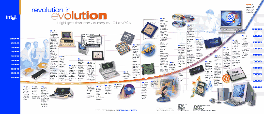
The development of microelectronics spans a time which is even lesser than the average life expectancy of a human, and yet it has seen as many as four generations. Early 60’s saw the low density fabrication processes classified under Small Scale Integration (SSI) in which transistor count was limited to about 10. This rapidly gave way to Medium Scale Integration in the late 60’s when around 100 transistors could be placed on a single chip.

It was the time when the cost of research began to decline and private firms started entering the competition in contrast to the earlier years where the main burden was borne by the military. Transistor-Transistor logic (TTL) offering higher integration densities outlasted other IC families like ECL and became the basis of the first integrated circuit revolution. It was the production of this family that gave impetus to semiconductor giants like Texas Instruments, Fairchildand National Semiconductors. Early seventies marked the growth of transistor count to about 1000 per chip called the Large Scale Integration.

By mid eighties, the transistor count on a single chip had already exceeded 1000 and hence came the age of Very Large Scale Integration or VLSI. Though many improvements have been made and the transistor count is still rising, further names of generations like ULSI are generally avoided. It was during this time when TTL lost the battle to MOS family owing to the same problems that had pushed vacuum tubes into negligence, power dissipation and the limit it imposed on the number of gates that could be placed on a single die.

The second age of Integrated Circuits revolution started with the introduction of the first microprocessor, the 4004 by Intel in 1972 and the 8080 in 1974. Today many companies like Texas Instruments, Infineon, Alliance Semiconductors, Cadence, Synopsys, Celox Networks, Cisco, Micron Tech, National Semiconductors, ST Microelectronics, Qualcomm, Lucent, Mentor Graphics, Analog Devices, Intel, Philips, Motorola and many other firms have been established and are dedicated to the various fields in VLSI like Programmable Logic Devices, Hardware Descriptive Languages, Design tools, Embedded Systems etc.

technology_evolution_timeline

Links:

Very Large Scale Integration (VLSI)

Very-Large-Scale-Integration_VLSI Gone are the days when huge computers made of vacuum tubes sat humming in entire dedicated rooms and could do about 360 multiplications of 10 digit numbers in a second. Though they were heralded as the fastest computing machines of that time, they surely don’t stand a chance when compared to the modern day machines. Modern day computers are getting smaller, faster, and cheaper and more power efficient every progressing second. But what drove this change? The whole domain of computing ushered into a new dawn of electronic miniaturization with the advent of semiconductor transistor by Bardeen (1947-48) and then the Bipolar Transistor by Shockley (1949) in the Bell Laboratory.

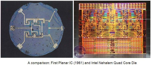
Since the invention of the first IC (Integrated Circuit) in the form of a Flip Flop by Jack Kilby in 1958, our ability to pack more and more transistors onto a single chip has doubled roughly every 18 months, in accordance with the Moore’s Law. Such exponential development had never been seen in any other field and it still continues to be a major area of research work.

VLSI_first_integrated_circuit_IC_compared_with_nehalem_quard_core_die

Links: